

Application 1: Infrared Spectrometer in Electronic Product Assembly Material Testing
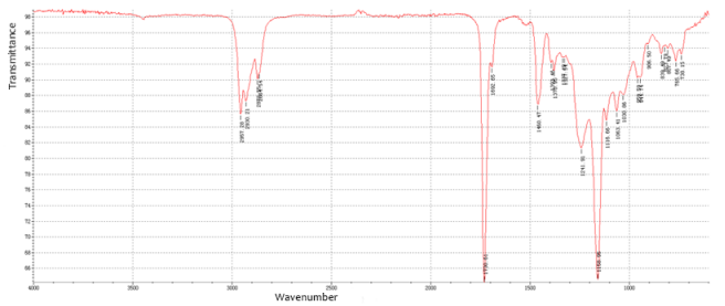
Electronic product assembly materials refer to raw or auxiliary materials used during the manufacturing process, such as adhesive tapes or glue for bonding, foam for insulation, protective films for safeguarding, or release films for lamination. The performance of these materials directly or indirectly impacts the quality of electronic products. Infrared spectroscopy (IR) can be used to conduct qualitative analysis of these materials.
|
Figure 1 Acrylic adhesive |
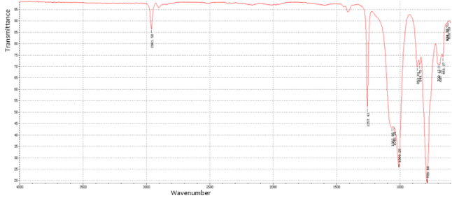 |
Figure 2 Silicone adhesive |
Application 2: Characterization of Coating Uniformity for Electronic Adhesives
Since most adhesives appear colorless and transparent after application, it is difficult to visually inspect the coating effect. Therefore, in practical use, a certain amount of fluorescent agent is added to the adhesive. The presence and uniformity of the adhesive coating are then checked by examining the fluorescence phenomenon of the coated product.
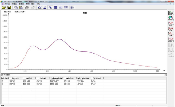
Using a molecular fluorescence spectrophotometer, the fluorescence emission spectrum of the product coated with adhesive (coating adhesive, conformal coating) is tested. By analyzing the spectrum to identify characteristic fluorescence peaks and comparing the fluorescence intensities of these peaks, it can be determined whether the sample has been coated with adhesive or whether the coating is uniform. This method is simple to operate and yields significant results.
|
| Figure 3 Overlay of Three Repeated Test Spectra |
Application 3: Qualitative or Semi-Quantitative Analysis of Phthalate Plasticizers in PVC and Other Plastics
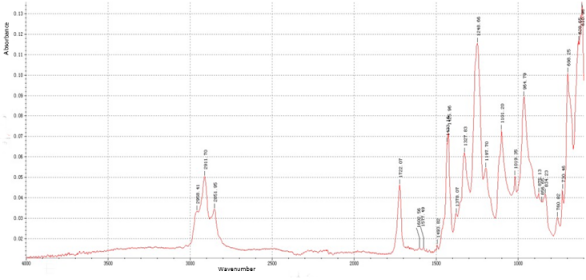
The EU's Directive (Restriction of Hazardous Substances) mandates that, starting from July 22, 2019, all electrical and electronic products (excluding medical and monitoring equipment) exported to Europe must comply with restricted limits for phthalate plasticizers. Among these, phthalate esters are widely used as plasticizers in electronic and electrical products.
|
| Figure 4 PVC containing a relatively small amount of phthalate |
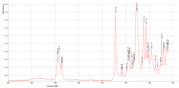 |
Figure 5 PVC containing a relatively large amount of phthalate esters |
Application 4: Qualitative Identification of Electrical Insulation Materials
Silicone rubber, with its exceptional properties including high and low temperature resistance, weather resistance, ozone resistance, corona resistance, and excellent electrical insulation performance, stands out as a uniquely versatile material among rubbers. It is particularly well-suited for use as organic insulation material in the electrical and power industries. In recent years, silicone rubber has seen increasingly widespread application in electrical insulation systems.
Most composite insulator manufacturers now utilize methyl vinyl silicone rubber filled with a high content of aluminum hydroxide as outdoor insulation material. Additionally, it is used as outer jacket insulation for composite lightning arresters, circuit breakers, transformers, high-voltage switches, and other electrical components.
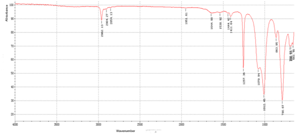 |
Figure 6 Silicone rubbers - raw rubber spectrum |
|
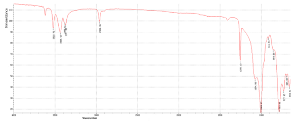
Figure 7 Silicone rubbers - finished product spectrum |
Application 5: Quantitative Analysis of Ink Curing Degree
With the widespread adoption of electronic devices, liquid crystal displays (LCDs) are being increasingly utilized, driving rapid growth in the LCD industry. UV-curable adhesives, a critical material in LCD production, offer fast curing speeds, solvent-free properties, and high production efficiency. They are primarily used for sealing and securing metal pins, making them widely applicable in the circuit board industry. In UV-curable adhesives, photoinitiators decompose rapidly into free radicals or cations under appropriate ultraviolet (UV) light intensity, triggering polymerization reactions of unsaturated bonds and resulting in material solidification.
|
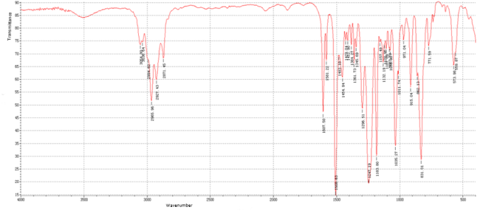
Figure 8 Epoxy Resin - Thermal Curing |
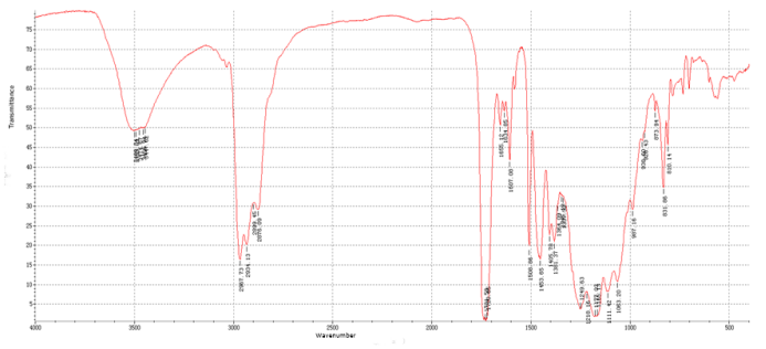 |
Figure 9 Polyacrylate - UV Curing |
Application 6: Optical Property Characterization of Semiconductor Materials (Transmission, Reflection)
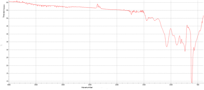
Semiconductor materials are among the most critical foundational materials in the electronics industry. With the rapid advancement of laser and infrared technologies, the exceptional optical properties of semiconductor materials in the infrared spectrum have garnered increasing attention. Today, materials ranging from elemental semiconductors like germanium (Ge) and silicon (Si) to compound semiconductors such as gallium arsenide (GaAs) and zinc selenide (ZnSe) are being widely utilized in infrared optical applications. These materials serve as essential components in forward-looking infrared (FLIR) systems, laser windows, missile domes, and other infrared optical systems.
|
Figure 10 Transmission Spectrum of Silicon Wafer |
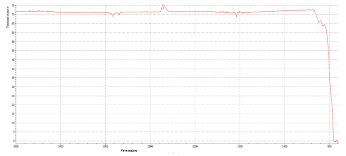 |
Figure 11 Transmission Spectrum of Zinc Selenide (ZnSe) |
Application 7: Material Identification for Electronic and Electrical Components
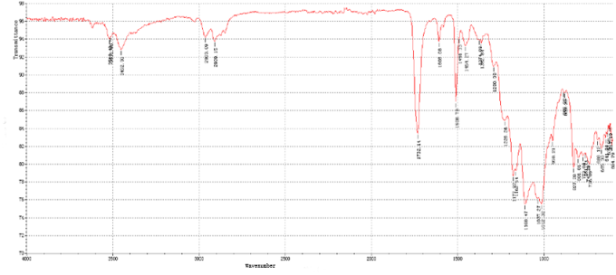
The substrates or enclosures of electronic products are typically manufactured using engineering plastics. These materials are formulated with specific additives such as reinforcing agents, flame retardants, and anti-aging compounds to meet various environmental requirements. The composition and proportion of these components critically determine the performance and lifespan of the final electronic parts. Infrared spectroscopy serves as an effective tool for qualitative analysis of these material compositions.
|
Figure 12 Epoxy Resin |
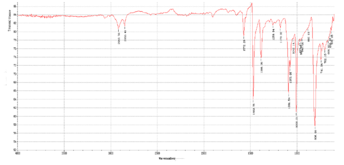
|
Figure 13 Polyphenylene Sulfide (PPS) |
Application 8: Testing of Electronic Product Packaging Materials
Electronic products are technology-intensive commodities. With continuous technological advancements, electronic components have evolved to ultra-large-scale integrated circuits, becoming increasingly sophisticated and complex. Consequently, their requirements for external environmental conditions have grown more stringent. As the protective and storage medium during circulation and storage, packaging's primary function is to safeguard electronic products. Only by ensuring rational structural design and high-quality packaging can electronic products be protected from moisture and mechanical shocks during transportation and storage, thereby preserving their appearance and functionality. Packaging materials serve as the foundation of packaging products. The appropriateness of their selection directly impacts both the safety of electronic products and economic costs. Therefore, selecting the right packaging materials is of critical importance.
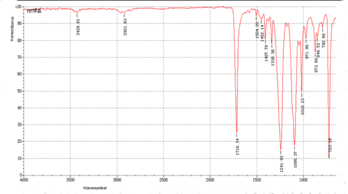
|
Figure 14 ATR Test Spectrum of PET Sample |
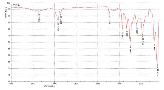
|
Figure 15 ATR Test Spectrum of PVC Sample |
Application 9: Defect Analysis of Electronic Products (Foreign Matter Analysis)
During the manufacturing process of electronic products, defects may occur. The qualitative identification and classification of these defects can help improve production processes and enhance product quality. However, these defects are typically micron-sized and cannot be detected using conventional analytical methods. By utilizing an infrared spectrometer equipped with an infrared microscope accessory, these minute defects can be effectively analyzed.
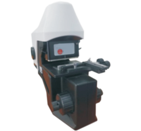
An infrared microscope is a system that combines an infrared spectrometer with an optical microscope. It primarily consists of an infrared main unit, an infrared microscope system, and a computer. Due to its precision, the infrared microscope predominantly operates on the principle of interference, with key components including a Michelson interferometer, microscope optical system, and detector.
The sample is placed on the stage of the infrared microscope. The spectrometer generates a beam that is directed and focused onto the sample, allowing for vertical focusing of the optical path. By adjusting the X and Y axes of the stage and the aperture, the specific sample and different micro-areas within the sample can be precisely targeted.
The infrared microscope detector measures the spectral reflectance of the particle beam, enabling molecular-level scanning of points, lines, and areas on the sample. This allows for the rapid and automated acquisition of numerous infrared spectra, with the coordinates of each measurement point and its corresponding infrared spectrum simultaneously stored in the computer. Through compositional image analysis, spatially resolved infrared spectra and compositional images of specific micro-areas can be obtained. This facilitates the analysis of the component and structural characteristics of the sample across various scanned micro-areas, thereby characterizing the sample's structure, spatial distribution of functional groups, and their variations.
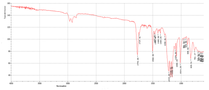 |
Figure 16 Conventional ATR Method |
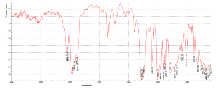 |
Figure 17 Micro-ATR Method |
Taking foreign matter on a laptop LED screen as an example, conventional single-reflection ATR accessories have limitations: shallow penetration depth, strong high-frequency absorption, weak low-frequency absorption, and inability to detect very small samples. In contrast, using the micro-ATR mode of an infrared microscope enables localized signal collection with deeper penetration depth and saturated signals in the corresponding spectral regions, allowing for the detection of samples smaller than 200 μm.